
Exclusive Design Feature
|
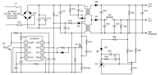
Don’t Let Jitter Shake Up Your Flyback Converter Designs Resonant ringing on the transformer primary can be the cause of harmless variation in the flyback converter’s duty cycle. However, if this side affect is not properly identified early in the design process, it may be misinterpreted as instability and lead to unnecessary and performance-degrading redesigns. One of the more popular topologies for startup and housekeeping power converters is the discontinuous-mode flyback converter with peak current-mode control. This topology is a favorite for converters producing 150 watts and below, because it enables small size, simplicity, and minimal magnetic components. Using the discontinuous, current-mode-contol configuration allows the flyback topology to have a simple and reliable feedback loop. A typical circuit for this type of application is presented in the schematic in Figure 1.
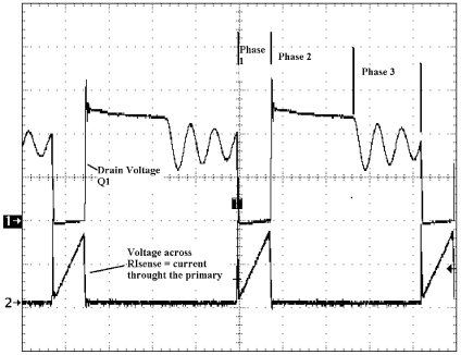
One of the issues that arises in the design of this converter is a variation in on-time (jitter) due to ringing on the transformer primary. If that jitter is erroneously attributed to instability, the designer may waste precious development time “correcting” the converter design. In some cases, the fix may even degrade converter efficiency. Fortunately, some simple tests can identify the transformer ringing as the source of the jitter. But before designers attempt to diagnose the jitter, it’s important to understand its origins. Modes of Operation In the discontinuous-mode, there are three states. All three occur within the time when the internal timer is completing a single cycle. The internal timer for the IC used in this example, a UCC38C44, is a saw tooth ramp generator. The first phase of the converter is initiated by turning on Q1, which starts at the same time that the ramp on the RT/CT pin starts to charge. The current in the primary winding of T1 starts to increase, resulting in a voltage being developed across RIsense. When this voltage reaches a peak, set by the feedback loop, the main switch is turned off and the inductive energy now stored in the primary inductance causes the voltage on the windings of T1 to reverse polarity. This is the beginning of the second phase. During this phase, the energy stored in the primary is delivered to the load in the form of current. This current will decrease linearly to zero. When the current hits zero, the circuit enters the third phase where the main switch is off and the transformer is not delivering energy to the output. This is characterized by a resonant ringing of the voltage across the primary winding. The three phases can be
easily seen in Figure 2, which shows both the voltage on Q1
and across RIsense.
A quick review of the requirements for a discontinuous flyback may be in order. For a fixed frequency converter operating at minimum input voltage and maximum load, the total “ON” time of the main switch plus the time needed to deliver energy to the load must be less than 100 percent of the available cycle time. To avoid having the power switch voltage on the drain ring below ground when the diode stops conducting at minimum input voltage, the reflected voltage on the primary should be less than the minimum input voltage. For a fixed load, primary inductance and frequency, the energy stored per cycle (hence the output load) is a function of the peak current, so the energy/power transferred to the transformer is:
The rate of the current’s change in the inductor’s primary is fixed for a fixed input voltage and primary (magnetizing) inductance:
In a stable circuit with a fixed input and output voltage, load and operating frequency, there should be a fixed and stable “ON” time to achieve a specific energy transfer. Parasitic components can result in slight variations to this ideal condition. These can give the appearance of instability in a stable circuit. To understand this, you have to look at the effect of the circuit
when the switching occurs. In particular, look at the voltage across
the main switch and the current in the inductor immediately after the
output diode stops conducting and just before the power switch turns
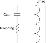
on. A simplified view of this circuit is shown in Figure 3
where Lmag represents the primary side magnetizing inductance, Csum
the collective parasitic capacitance, and Rwinding the effective
winding resistance.
At this point, the circuit is an L-R-C series resonant circuit (where Csum is the sum of the total capacitances across the windings) that is charged to the reflected output voltage with a dc offset equal to the input voltage. The reflected output voltage is across Lmag. This circuit will ring at a frequency set by the inductance, Lmag and the capacitance, Csum according to Formula 3:
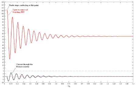
Since one terminal of the transformer is connected to the input voltage, the circuit will have a dc offset equal to Vin. The waveform will decay as a function of the losses represented by Rwinding. A representative voltage and current waveform is shown in Figure 4.
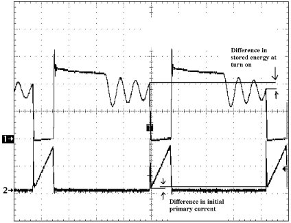
Figure 4 shows the voltage waveform on the drain of the switching FET and primary winding current. These waveforms show the end of Phase 2 and the beginning of Phase 3. The voltages, currents and time in Figure 4 are representative and are not to scale. If the time between the diode conducting and the main switch turning on is long enough, the ringing dies out and there is no perceptible jitter. However, if the time is short and significant ringing is still present at the start of the next Phase 1, there may be jitter. This is the case for the waveforms of Figure 2 and shown in
Figure 5.
The ringing represents the oscillating current and voltage within the transformer’s primary winding. Ignoring losses and referring to Figure 3, the energy in the system is initially represented by the maximum voltage across the capacitance. This energy will be converted to current through the inductance over the resonant ring cycle. This conversion results in the maximum current through the winding according to the following equations where E is the total energy in the system. At any point on the ring waveform (different Vs and different Imags), the sum of the Formulas 4 – 5 (ignoring losses) should be E:
If V is the effective instantaneous voltage across the primary winding at the point where the output diodes stop conducting, the Imag is the effective current through the magnetizing inductance, Lmag. When the voltage across the winding is ringing through the zero point, the above formulas represent the maximum voltage and currents within the closed circuit. Depending on the direction of the ring, that current can be negative or positive. So according to these formulas, depending on the point in the ring cycle you will have different effective currents in the primary winding. This results in different residual currents in the primary winding. Thus, if the main switch turns on at different starting points on the ring cycle, the circuit will have different starting points on the current ramp. Since the starting point from cycle-to-cycle can be different, the time to reach the same peak current can be different, thus the “ON” time is different. The time when the converter’s main switch turns on is set by a separate R/C oscillator as described earlier, so there is a fixed time per cycle. The time to transfer the energy to the secondary is fixed by the output voltage and the magnetizing inductance, which do not change. The remaining time now has a slight variation because of the slight variation in the “ON” time, so now there will be a slight variation in the ring time. This is shown in Figure 5 by the point on the ring voltage waveform, where Phase 3 ends and Phase 1 begins. This results in the instantaneous current in the primary having slight variations from cycle to cycle. This difference is shown in Figure 5 by the difference in the initial voltage on the current sense resistor at the beginning of Phase 1. It is this behavior that leads to the variations in the “ON” time. This variation in duty cycle can be misinterpreted as a stability issue and result in extensive work to try to remove the problem. A quick way to check this is to either increase or decrease the input voltage. This will result in the ringing moving toward a peak or valley when the main FET turns on as the input voltage changes. This should result in a decrease in the amplitude of the jitter and, as you get to the other side (down slope) of the waveform for the transition, the effect tends to negate the jitter entirely as any change results in less change on the next cycle. Conclusion Minimizing the parasitic capacitance limits the current in the winding, increases the ring frequency and reduces the above described effect, as the stored energy will be decreased. If you add damping elements to minimize the ringing, this results in increased losses. Since the jitter is not a result of instability and can be explained, it should be safe to ignore it after recognizing the cause.
References To download a datasheet or other technical documents for the UCC38C44, visit: www.ti.com/ucc38c44-ca. For more information about power solutions from Texas Instruments, visit: www.ti.com/power-ca. About the Author
For further reading on flyback converter design, see the How2Power Design Guide. |
 John Bottrill is a
Senior Applications Engineer at Texas Instruments, Manchester, NH.
John supports customers and evaluates new ICs before release. Through
this process, he has published multiple technical papers and has two
patents to his credit. He received his B. Sc. in Electrical
Engineering from Queen’s University at Kingston, Ontario,
Canada. You can reach John at
John Bottrill is a
Senior Applications Engineer at Texas Instruments, Manchester, NH.
John supports customers and evaluates new ICs before release. Through
this process, he has published multiple technical papers and has two
patents to his credit. He received his B. Sc. in Electrical
Engineering from Queen’s University at Kingston, Ontario,
Canada. You can reach John at